Neural Network Dependability Kit (Fortiss)

Information

Partner: FORTISS, MUNICH, GERMANY
Advanced Technology: Neural Network Dependability Kit
Contact: Dr. Holger Pfeifer
Email: pfeifer@fortiss.org

Neural Network Dependability Kit

A toolbox to support safety engineering of artificial neural networks

In recent years, neural networks have been widely adapted in engineering automated driving systems with examples in perception, decision-making, or even end-to-end scenarios. As these systems are safety-critical in nature, problems during operation such as failed identification of pedestrians may contribute to risk behaviours. Importantly, the root cause of these undesired behaviours can be independent of hardware faults or software programming errors but can solely reside in the data-driven engineering process, e.g., due to unexpected results of function extrapolation between correctly classified training data.

The Neural Network Dependability Kit (NN-dependability-kit) is an open-source toolbox to support safety engineering of neural networks. It supports verification, test-case generation and metrics computation for neural networks. The key functionality includes:

  • Formal reasoning engine for ensuring that the generalization does not lead to undesired behaviours, and
  • Novel dependability metrics for indicating sufficient elimination of uncertainties in the product life cycle

  • Runtime monitoring for reasoning whether a decision of a neural network in operation time is supported by prior similarities in the training data.

The NN-dependability-kit is available for download at GitHub, where further information can be found: https://github.com/dependable-ai/nn-dependability-kit

Examples of NN-dependability-kit use cases:

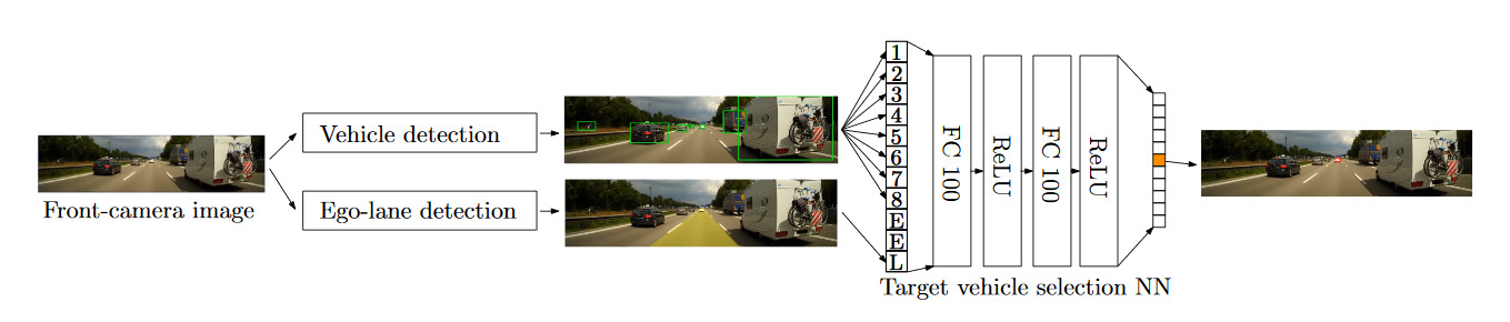
  1. Formal Verification of a Highway Front Car Selection Network

Formally verifying properties of a neural network that selects the target vehicle for an adaptive cruise control (ACC) system to follow. The overall pipeline is illustrated in the figure, where two modules use images of a front facing camera of a vehicle to (i) detect other vehicles as bounding boxes and (ii) identify the ego-lane boundaries. Outputs of these two modules are fed into the third module called target vehicle selection, which is as a neural-network based classifier that reports either the index of the bounding box where the target vehicle is located, or a special class for “no target vehicle”.

The input features of the Target vehicle selection neural network are defined as follows: 1-8 (possibly up to 10) are bounding boxes of detected vehicles, E is an empty input slot, i.e., there are less than ten vehicles, and L stands for the ego-lane information.

A tutorial for this example is available at the GitHub repository: https://github.com/dependable-ai/nn-dependability-kit/blob/master/TargetVehicleProcessingNetwork_FormalVerification.ipynb

  1. Perturbation Loss over German Traffic Sign Recognition Network

Analysing a neural network trained under the German Traffic Sign Recognition Benchmark with the goal of classifying various traffic signs. With NN-dependability-kit, one can apply the perturbation loss metric, in order to understand the robustness of the network subject to known perturbations.

A tutorial for this example is available at the GitHub repository: https://github.com/dependable-ai/nn-dependability-kit/blob/master/GTSRB_AdditionalMetrics.ipynb

π-Fab infrastructure (FhG)

Information

Partner: Fraunhofer IISB
Advanced Technology: π-Fab infrastructure
Contact: Markus Pfeffer
Email: Markus.Pfeffer@iisb.fraunhofer.de

π-Fab infrastructure FRAUNHOFER (FhG)

π-Fab – Low Volume Prototype Fabrication of Customized Electron Devices

Device development conducted at our institute can be transferred into a small-volume manufacturing process by ISO 9001 certified “π-Fab”. π-Fab is a joint collaboration between the Fraunhofer IISB and the Chair of Electron Devices dedicated to the realization of prototype devices under an industry-compatible fabrication environment. Fabrication ranges from single process steps across process modules up to full-fledged device fabrication including Statistical Process Control and Process Control Measurements on calibrated measurement tools. Additionally, electrical characterization for 100% device testing is available. These activities allow for the first phase of a product ramp-up when fabrication capacities by foundries – due to non-standard CMOS technology requirements – or the global players in power device fabrication are not yet available due to the low production values.

π-Fab facts:

  • P rocess line based on 0.8 µm CMOS technology
  • Wafers: Si, SiC, and others
  • Wafer sizes: samples to 200 mm
  • Devices
    • CMOS
    • Power
    • Sensors
    • MEMS
    • Passives

For more information:

Markus Pfeffer
Fraunhofer IISB, Erlangen, Germany
Markus.Pfeffer@iisb.fraunhofer.de
https://www.iisb.fraunhofer.de/
https://eurocps.org/design-centers/fhg-germany/

4Diac (Fortiss)

Information

Partner: FORTISS, MUNICH, GERMANY
Advanced Technology: Framework for Distributed Industrial Automation & Control
Contact: Dr. Holger Pfeifer
Email: pfeifer@fortiss.org

Framework for Distributed
Industrial Automation & Control

Today’s automation and control systems are mostly implemented according to a vendor specific dialect of the IEC 61131 standard. The different dialects make programs for programmable logic controllers (PLC) hardly portable between different PLCs. With its PLC centric design and its scan-based nature, the IEC 61131 standard already exceeds the needs of today’s automation systems. Therefore the same standardization group, originating IEC 61131, worked on a more flexible version, supporting distributed automation and control systems, the IEC 61499 standard.

IEC 61499 based systems follow an application centric design, which means that the application of the overall system is created at first and independent of the hardware. Each application is created by interconnecting the desired function blocks (FB) in terms of a function block network (FBN). The IEC 61499 standard extends the FB concept, already introduced within the IEC 61131 standard by an event interface, which allows an explicit definition of the execution order. This is required especially for distributed systems.

As soon as the hardware structure is known it can be added to a project’s system configuration and the already existing application can be distributed onto the available devices. The interoperability of devices from different vendors is one key feature postulated by the IEC 61499 standard. Also the portability of applications between different IEC 61499 engineering tools has been addressed by introducing an XML exchange format. Due to the definition of management commands different devices can be configured by different IEC 61499 engineering tools. The same commands can be used for online reconfiguration.

Eclipse 4diac™ implements the IEC 61499 standard and is intended for the programming of programmable logic controllers (PLCs) as well as small embedded control devices. 4diac is provided as open source software under EPL-1.0 and consists of two parts: forte (4diac-rte) and 4diac-ide.

  • forte is a real-time capable IEC 61499 run-time, which operates on different hardware platforms. The hardware platforms reach from small embedded control devices up to PLCs. Currently supported hardware platforms comprise e.g. Weidmüller PLC, Wago PLC, Raspberry Pi, BeagleBone Black, or LEGO Mindstorms NXT. forte has been tested on e.g. Windows Cygwin on i386, ppc and xScale Linux on i386, ppc and xScale NetOS RTOS on IPC@chip and eCos on ARM7. It supports all IEC 61131-3 edition 2 elementary data-types, structures, and arrays. Applications can consist of any IEC 61499 element as basic function blocks, composite function blocks, service interface function blocks and adapters. Besides that forte provides a flexible and extendable communication infrastructure already providing a large set of protocols, e.g. MQTT, OPC UA, openPOWERLINK or EclipseSCADA.
  • 4diac-ide is an extensible, Eclipse-based integrated development environment (IDE) for IEC 61499 compliant programs. It supports the modelling of distributed control software as well as the deployment to the various hardware devices. 4diac-ide makes it easy to create new applications in a modular way by reusing existing function blocks from standard libraries. The modelled applications can be deployed to IEC 61499 powered control devices. For testing, 4diac-ide provides monitoring and debugging facilities to “watch” events and data values during execution. One can also interact with the application by changing or forcing data to have certain values, and by triggering events.

4diac has been evaluated by case studies of different organizations:

  • The Profactor Case Study. Profactor is located in Steyr, Austria and is Austrian’s No. 1 in applied production research. As a private research company, it performs applied research across different disciplines to find solutions for the manufacturing industry. The Profactor case study employed the 4diac platform on a robotic arm application.
  • The AIT Case Study. The AIT (Austrian Institute of Technology) is Austria’s largest non-university research institute, and among the European research institutes a specialist in the key infrastructure issues of the future. In this case study AIT examined the use of the 4diac platform in a smart grid laboratory.
  • The ACIN Case Study. Vienna University of Technology – Automation and Control Institute (ACIN) performs research and education in the fields of distributed automation and control systems, as well as precision engineering, scientific instrumentation and process-measurement systems with focus on industrial relevant applications for industrial automation, production, and measurement systems. The ACIN case study allowed the Vienna Institute of Technology’s Automation and Control Institute to demonstrate the real time capability of the 4diac platform.
  • Awite Bioenergie GmbH. Awite is a SME located near Munich and is specialist for gas analysis and desulfurization as well as the automation of the corresponding processes. Within their CPSE Labs Experiment they implemented an energy load management approach with 4diac. They summed up their results within a YouTube video.

For more info please contact

Dr. Holger Pfeifer

Email: pfeifer@fortiss.org

https://www.fortiss.org/home/

AIDE (KTH)

Information

Partner: KTH, Sweden
Advanced Technology: AIDE Data management tools
Contact: Jad El-khoury
Email: jad@kth.se

AIDE: Data management tools for the engineering of CPS

The development of Cyber-Physical Systems (CPS) includes multiple experts from different disciplines. This implies that there will be multiple sets of system descriptions that jointly describe the entire system including its design and verification (compare with software, electronics hardware, communications, mechanical packaging, reliability and safety engineering).

CPS development will thus typically be characterized by fragmented product descriptions such as requirements, design descriptions, models, source code, hardware descriptions, configuration data, etc. All these fragments will be stored and managed through a number of tools and databases. Since these fragments are interrelated, it is important to be able to relate them to each-other, to keep them consistent, and to understand how a change in one artefact impacts other – and in an efficient way. A typical example is to be able to find test-cases corresponding to a particular requirement.

To address this problem, the overall objective of AIDE is to lower the threshold of integrating and managing data among software tools, thereby improving end-user processes, in turn with potential for improvements in time to market, more effective use of resources and product quality. This is accomplished by providing support tools – for creating tailored “tool-chains” and integrations of data for the engineering of CPS. The approach targets data integration based on open standards (such as OASIS OSLC, and the Linked Data family of standards) and open source software. Fig. 1 illustrates the scene of fragmented data/tools and how making data available opens up possibilities to create added value services. The focus of the existing AIDE support tools is indicated by the red encirclement.

AIDE software assets:

As an integral part of the open-source OSLC Lyo project, Lyo Designer is a tool that supports architects and developers with the architecting, design and implementation of integrated tool chains, compliant with the OSLC standard. Lyo Designer consists of a toolchain modelling tool, and an accompanying code generator that produces OSLC-compliant tool adaptors, integrating the designed tools.

Lyo Designer complements the Lyo SDK – the set of Java libraries that helps the community adopt OSLC specifications and build OSLC-compliant tools.

AIDE’s tool support also includes a number of open source components which have been developed with a number of partners over the years such as

What are typical use cases

Lyo Designer has been used and validated by a range of industrial partners. Moreover, since its release, close collaboration with external partners (Ericsson, FindOut, IBM, OFFIS, Scania, Thales and Volvo) have been established. These partners are using as well as extending the platform in coordination with KTH.

As indicated by Fig. 1 and the red encirclement, there are several opportunities to extend the current capabilities of the AIDE Lyo Platform. At KTH in collaboration with industrial partners we are currently pursuing work in the following directions:

  • Supporting the operational phase of cyber-physical systems through interfaces for data gathering from operational CPS and for controlling such CPS. This includes concepts such as digital twins.
  • Data warehousing facilities, in which a protocol is being implemented and extended that allows for the real-time communication of operational data across a CPS.

How easy is it to use it and what about gaining access?
The AIDE assets target toolchain architects and developers of tool interfaces. The adopted model-based approach aims to lower the threshold of adopting the OSLC standard for industrial developers. Lyo Designer allows one to work at a higher level of abstraction, with models to specify the overall architecture as well as specific tool designs, without needing to deal with all the technical details of the OSLC standard (such as Linked Data, RDF, etc.). Its accompanying generator also helps in the rapid prototyping of the tool interfaces.

Most of AIDE’s software assets are part of the Eclipse Lyo project, and are released under the EPL license. Details of the Lyo project can be found under its Wiki pages (https://wiki.eclipse.org/Lyo).

Where can I find more information?

A full description of the AIDE assets can be found here:

Further information and support can be obtained from KTH – see contacts.

Contacts:

Jad El-khoury (KTH), jad@kth.se

Martin Törngren (KTH), martint@kth.se

Advanced nanotechnology for chemical sensing (CSEM)

Information

Partner: CSEM
Advanced technology: Advanced nanotechnology for chemical sensing
Contact: Guy Voirin
Email: guy.voirin@csem.ch
Tel: +41 032 720 5152

Advanced nanotechnology for chemical sensing

From nanotechnology to sensing applications
From nanotechnology to devices

WHAT IS our technology

The miniaturization of sensors together with the dramatic increase in portable computational power is currently generating a wide range of new applications for chemical sensors. These sensors can be used for applications related to environmental, health, aeronautics, or even food safety monitoring just to name a few. In order to be used with portable devices, sensing materials must be small, cost effective, and reliable. Sensors based on luminescence changes in the presence of specific molecules are promising candidates for this type of applications as these sensors can be interrogated with standalone compact optical readers that have wireless communication capabilities. CSEM has developed new optical sensitive patches based on a sol-gel nanoporous layer and these luminescent films are adapted for O2, CO2, and pH detection.

Nanotechnology based sensitive layers:

To make the most of the photosensitive dyes, new functionalized thin films based on nanoporous layers have been developed and can be deposited on various substrates such as steel, glass, and flexible plastic sheets. The host film is made of a double matrix: a microporous sol-gel network encapsulating the active dyes, which is embedded in a mesoporous coating. This hierarchical nanostructure brings enhancement to the sensing layers properties, such as optical signal, sensitivity, robustness, mechanical resistance, transparency, selectivity, and response time.

These nanoparticle based layers can also be deposited on MEMS structures to build sensors (electrical, electrochemical) using the nanoporous layer as a catalyst for sensing materials.

APPLICATIONS

Miniaturization of sensors for different connected applications

  • Oxygen sensing in pressure sensitive paint (PSP)
  • Oxygen sensing in cell culture, air quality, water quality, and breath monitoring
  • Carbon dioxide sensing in buildings, food packaging, food preservation, and breath monitoring
  • Carbon dioxide, oxygen, and pH sensing for water quality (rivers, swimming pools)
  • VOC for buildings, cars

What’s new?

  • Patented technology (EP 3184994, US 2017176332)
  • Deposition of the sensing layer with high resolution on structured or fragile substrates (membranes)
  • Reversible and disposable sensors for continuous monitoring
  • O2 sensing capabilities with accuracy <0.2%, range 0-21%, and precision 0.3%
  • CO2 sensing capabilities with accuracy 0.2%, range 3-12%, and precision <1%

WHAT’s NEXT

  • Customization of sensor integration for extending the range of application
  • Wearable sensors for health monitoring
  • Adaptation of the sensing layer to new chemicals

INTERNATIONAL RECOGNITION:

FOR MORE INFORMATION

Contact: Guy Voirin
Email: guy.voirin@csem.ch
Tel: +41 032 720 5152

Advanced manufacturing/packaging (CSEM)

Information

Partner: CSEM
Advanced technology: Advanced manufacturing/packaging
Contact: Sébastien Lani
Email: sebastien.lani@csem.ch
Phone: +41 032 720 5535

Advanced manufacturing/packaging

Smooth and vertical surfaces

High design flexibility

Conductive ink deposition on 3D molded surfaces

Open fluidic package with silicon based micro porous membrane

Closed fluidic package demonstrating liquid tightness with no glue

MEMS overmoulding with integrated electrical leads

Combination of additive manufacturing and microfabrication

WHAT IS our technology

Combination of several 2/3 D printing technologies with microfabricated elements

  • UV stereolithography (UV SLA):
  • UV polymerization of a liquid resin by projection of patterns (layers) generated with a DLP projection system
  • Layers from 5 to 100μm
  • Minimum object size: 50μm (polymer hard)
  • Accuracy from 10 to 20μm
  • Material: polymer, ceramic (SiO2 based and SiC)
  • Build volume: up to 102 x 57.5 x 120mm3
  • Printing on substrate possible
  • Alignment camera

Fuse Filament Fabrication (FFF)

  • Printing of fused polymer like extrusion
  • Large variety of polymer: PET, ABS, PLA, PVA, nylon, composites (ceramics, conductive, magnetic…), fiber reinforced polymer (carbon, glass fiber)
  • Minimum layer of 20μm. Typical layer thickness comprised between 60 and 100μm
  • Minimum wall thickness of 0.5 to 0.8mm
  • Printing on substrate possible

Aerosol Jet Printing

  • Aerosol-jet printer system AJ-300 from Optomec
  • Table 300 x 300 mm2 (+/- 6 micron accuracy)
  • Heated vacuum platen
  • 2 atomizers: Pneumatic (PA) and Ultrasonic (UA)
  • Nozzles from 150μm to 1mm
  • Alignment camera
  • Deposition of liquid solution from 1 to 1000cP

Hybrid platform

  • 2 FFF head
  • Droplet dispensing
  • Syringue dispensing
  • UV LED
  • IR laser

APPLICATIONS

For Smarter components and System Integration

  • 3D electrical connections
  • Integrated sensors
  • Identification or decoration
  • Shock or vibration absorbers
  • Smart prosthesis and implant
  • Antenna
  • Microfluidics and bioreactors

What’s new?

Alignment possibilities with MEMS.

WHAT’s NEXT

Complete system integration.

INTERNATIONAL RECOGNITION:

Several publications and references in international journals and conferences

FOR MORE INFORMATION

Contact: Sébastien Lani
Email: sebastien.lani@csem.ch
Tel: +41 032 720 5535

Soft MEMS (CSEM)

Information

Partner: CSEM, Switzerland
Advanced technology: Soft MEMS
Contact: Guy Voirin
Email: guy.voirin@csem.ch
Phone: +41 032 720 5152

Soft MEMS

Development of a fully soft sensor

WHAT IS our technology

Stretchable soft membranes that can be integrated on MEMS structure to realize:

  • Platform for direct measurement of movements and forces of individual cells
  • Platform to measure Young’s modulus of a confluent cell layer
  • Strain gauge integrated in soft membrane
  • Si sensors/electronics integrated into soft membranes
  • Actuator based on SI or LTCC (Low Temperature Co-fired Ceramics) technologies with PDMS (Polydimethylsiloxane) micro valves.

CellStrates Project

APPLICATIONS

  • Strechable membranes for study of cell’s mechanics
  • Monitoring of cell traction
  • Measurement tool at CellStrates (http://cellstrates.com/)
  • Interactive refreshable graphical display for tactile applications (Braille like display)
  • Artificial skin with flexible metal interconnections and strain gauge for miniature tactility sensors and haptic applications

Braille like display project

What’s new?

  • Implanted strain sensor into stretchable membrane
  • Hermetic sealing between soft and hard material

WHAT’s NEXT

A fully integrated components with sensors, actuators based on stretchable soft membrane to develop a glove with articicial sensitive skin.

INTERNATIONAL RECOGNITION:

Sorba, F. and Martin-Olmos, C., 2018. High resolution polymer coated strain sensors for in-liquid operation. Microelectronic Engineering, 191, pp.38-41.

FOR MORE INFORMATION

Contact: Guy Voirin, guy.voirin@csem.ch
Contact: Cristina Martin-Olmos, cristina.martinolmos@csem.ch

WiseMAC (CSEM)

Information

Partner: CSEM
Advanced technology: WiseMAC
Contact: Philippe Dallemagne
Email: philippe.dallemagne@csem.ch
Phone: +41 032 720 5521

WiseMAC

Peer to Peer low power medium access protocol for wireless communication.

WHAT IS WiseMAC?

WiseMAC is a peer-to-peer MAC protocol for wireless communication that allows ultra-low-power operation with low latency. It is based on an adaptive preamble sampling and does not require any network synchronization. It may be used to construct multi-hop networks with battery-operated routers. In star networks, it outperforms most protocols in terms of downlink latency (sensor parametrization or actuator update) with similar uplink performances.

WiseMAC:

  • Asynchronous MAC protocol for wireless networks
  • does not require any setup signalling
  • is completely asynchronous and does not rely on any network wide synchronization
  • outperforms IEEE 802.15.4 (ZigBee/Threads/…) and most low power protocols both in terms of power consumption and latency
  • ultra-low-power peer-to-peer communications with low latency
  • supports multihop networking with battery operated routers
  • optional multichannel operation for safety and dependable operations
  • available on COTS devices (incl. 802.15.4 transceivers) and CSEM SoCs.

APPLICATIONS

  • Safety (e.g. ship evacuation, avalanche detection)
  • Building control & surveillance
  • Environment (e.g. water quality monitoring)
  • Agriculture (e.g. vineyards)
  • Smart homes / home automation
  • Asset tracking, people / patients monitoring and more…

What’s new?

  • No configuration
  • Ultra-low-power peer-to-peer operations (on both peers)
  • Smoothly adapts to varying traffic from very low to medium
  • Low latency sensor configuration and actuator update in star mode

WHAT’s NEXT

Further energy reduction through adaptation

INTERNATIONAL RECOGNITION:

Numerous publications and references in international journals and conferences.

FOR MORE INFORMATION

Contact: Philippe Dallemagne

Email: philippe.dallemagne@csem.ch

Tel: +41 032 720 5521

Localization Solver (CSEM)

Information

Partner: CSEM, Switzerland
Advanced technology: Localization Solver
Contact: Martin Sénéclauze
Email: martin.seneclauze@csem.ch
Tel: +41 32 720 53 40

Localization Solver

A GPS Free Generic Radio Localization Solver.

WHAT IS A GPS FREE LOCALIZATION SOLVER?

The aim of the positioning solver is to allow localization of any communicating device in a reliable manner whether indoor or outdoor. Based on the information collected directly from the radio, the solver is capable of parsing, filtering and analysing the transmission quality to integrate a reliable position.

Tailored around a particle filtering technique, information collected from the radio environment is transformed into a series of possible points, called particles. For each of these particles, a probability of being the searched position is calculated. The probabilities of all particles are processed through an iterative process until convergence.

CSEM GPS FREE LOCALIZATION ALLOWS:

  • Localization of any objects communicating wirelessly provided infrastructure.
  • Integration with any type of radio capable of generating RSSI, SNR, ToF, AoA, TDoA, DTDoA (LoRa® / LTE-M / NB-IoT / WiFi / BT or customised hardware)
  • Tracking devices without modifying the infrastructure nor the hardware allowing low power localisation
  • Easy port to handheld device or cloud servers (AWS, Microsoft Azure, …)
  • Early data fusion to integrate obvious data rejection (Map Matching …)

APPLICATIONS

  • Logistics, Security
  • Pets / Objects / People Tracking / Finding
  • Occupancy detection
  • Drone navigation and obstacle avoidance
  • Planification

What’s new?

  • By using random based initial distribution, the caveats of the generally used geometrical calculation is greatly reduced (less impact of local minima)
  • Solver was intensively tested on LoRa® network and RSSI with results 10 to 50% better than evaluated competition

WHAT’s NEXT

CSEM will continue to develop its GPS Free Localization Solver to improve its level of precision. The next path to be evaluated is the usage of Machine Learning to discriminate bad measurements and limit the impact of multipath.

Depending on the need of our partners, we are introducing probability based constraints to early adapt to other types of information like proximity, room, path …

FOR MORE INFORMATION

Contact: Martin Sénéclauze
Email: martin.seneclauze@csem.ch
Tel: +41 32 720 53 40

Hyper Vision (CSEM)

Information

Partner: CSEM
Advanced technology: Hyper Vision
Contact: Andrea Dunbar
Email: andrea.dunbar@csem.ch
Phone: +41 032 720 5069

Hyper Vision

Intelligent Camera System for Hyper-spectral Imaging.

WHAT IS THE HYPER VISION SYSTEM?

CSEM offers a hyperspectral imaging system based on a new idea of light-field imaging. With low cost, the hypercube resolution of the camera is offering best-in-class performance. Also, the camera has a modular structure which enables us to easily customize it for different applications and environments. It offers flexibility in spatial resolution and in spectral channels.

HYPER VISION SYSTEM:

Characteristics
Number of Spectral Channels 54 (customizable)
Wavelength Range (nm) 450 – 880 (customizable)
Spectral Resolution (nm) 12
Cube Resolution (pixel) 280 × 280 × 54 (customizable)
Detector Type Si CMOS
Shutter Type Global Shutter
Camera Interface USB 3.0

APPLICATIONS

  • Process control
  • Medical diagnostics
  • Precision agriculture
  • Food quality

What’s new?

  • Modular system
  • Customizable spatial resolution
  • Customizable number of channels
  • Customizable wavelength range
  • Adaptive: ability to trade spatial and spectral resolution
  • Machine learning for information extraction and classification

WHAT’s NEXT

  • Tailoring the camera for specific applications by using only the spectral channels that are relevant for each application. This is possible due to modularity and high customizability of the design.
  • Miniaturizing the camera to be portable on the drones
  • Embedding the machine learning unit for binocular-type applications.

INTERNATIONAL RECOGNITION:

  • 2 patent applications

VIDEO Overview

Link to video: https://www.youtube.com/watch?v=OwhdnpQiaas

FOR MORE INFORMATION

Contact : Andrea Dunbar
Email : andrea.dunbar@csem.ch
Tel : +41 032 720 5069

Click here to add your own text