
Information
| Partner: | Fraunhofer IISB |
| Advanced Technology: | π-Fab infrastructure |
| Contact: | Markus Pfeffer |
| Email: | Markus.Pfeffer@iisb.fraunhofer.de |
π-Fab infrastructure FRAUNHOFER (FhG)
π-Fab – Low Volume Prototype Fabrication of Customized Electron Devices
Device development conducted at our institute can be transferred into a small-volume manufacturing process by ISO 9001 certified “π-Fab”. π-Fab is a joint collaboration between the Fraunhofer IISB and the Chair of Electron Devices dedicated to the realization of prototype devices under an industry-compatible fabrication environment. Fabrication ranges from single process steps across process modules up to full-fledged device fabrication including Statistical Process Control and Process Control Measurements on calibrated measurement tools. Additionally, electrical characterization for 100% device testing is available. These activities allow for the first phase of a product ramp-up when fabrication capacities by foundries – due to non-standard CMOS technology requirements – or the global players in power device fabrication are not yet available due to the low production values.
π-Fab facts:
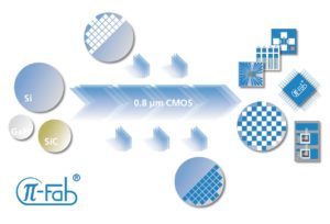
- P rocess line based on 0.8 µm CMOS technology
- Wafers: Si, SiC, and others
- Wafer sizes: samples to 200 mm
- Devices
- CMOS
- Power
- Sensors
- MEMS
- Passives
For more information:
Markus Pfeffer
Fraunhofer IISB, Erlangen, Germany
Markus.Pfeffer@iisb.fraunhofer.de
https://www.iisb.fraunhofer.de/
https://eurocps.org/design-centers/fhg-germany/